
Micro Vias Affect the Manufacturability
The manufacturability of a rigid-flex PCB depends in large part on the quality of its microvias. These small holes are the electrical pathways between layers in the board, and their design impacts all aspects of the circuit’s performance, including thermal management, power handling capabilities, and mechanical stability. As such, micro vias require careful consideration when designing a PCB.
The most critical aspect of a PCB’s micro vias is the materials that are used to construct them. The choice of fill and plating materials is essential, and must be chosen with a careful eye for the impact on the microvias’ electrical and thermal properties. In addition, the metallization process is crucial to the microvias’ overall reliability. It must be conducted under carefully controlled temperatures and with consistent micro coverage to ensure reliable electrical connections between the layers of a PCB.
While the benefits of using microvias can be considerable, they are not without their drawbacks. The process of constructing them is highly complex, with stringent manufacturing requirements. This can create difficulties for less-advanced manufacturers. In addition, microvias are prone to failure after a high number of thermal cycles. This is a result of the small size and high thermal expansion of the microvia’s material.
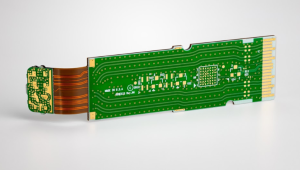
How Do Micro Vias Affect the Manufacturability of Rigid-Flex PCBs?
As such, it is important to choose a fabricator with experience in manufacturing rigid-flex PCBs that include microvias. An experienced fabricator will understand the issues associated with incorporating these small features into a design, and be able to suggest modifications that improve manufacturability.
Defining the PCB stackup using a tool like PCB Stackup Editor is the first step in ensuring manufacturability of a PCB with microvias. This will help you to select the right laminates and define layer pairs, while ensuring that your fabrication processes can accommodate these small features. Once you’ve defined a proposed stackup, I recommend sending it to your fabricator for review and input as to whether it will be manufacturable with microvias.
Once the PCB stackup is a good fit for your manufacturing process, it’s time to begin drilling the required number of microvias. Rigid-flex manufacturers drill these tiny holes with ultra-high speed tools, typically utilizing Excimer YAG or CO2 lasers to make precision holes in the copper laminate. This is followed by etching the circuit pattern, which converts the copper layer into the desired PCB structure.
Microvias may be stacked in a single plane (with the same center position on both X and Y coordinates) or staggered in a single plane to save space. Staggered construction allows designers to take the drilling positions away from overcrowded areas of the copper plane and spread them out to less impacted areas.
After drilling and etching, the microvias must be filled and plated with a conductive material. This is usually done with copper, and it’s important to use a consistent metallization process to maintain consistent microvia wall coverage. The plating process also helps to reduce the risk of shorts caused by differences in electrical resistance between adjacent microvias.