
RF circuit boards ensure low signal attenuation
Signal attenuation is the gradual loss of signal strength as it travels through a transmission medium, and it is a significant concern in RF (Radio Frequency) circuit boards. High levels of attenuation can result in poor signal quality, reduced range, and ineffective communication, especially in wireless systems like mobile networks, satellite communications, and IoT devices. RF circuit boards are specifically designed to minimize signal attenuation, ensuring that signals maintain their strength and integrity as they pass through the circuit. Various strategies, from material selection to careful layout design, are employed to reduce signal loss and achieve optimal signal performance.
One of the most critical factors in reducing signal attenuation in rf circuit board is the material used in their construction. The dielectric material—the insulating layer between the conductive traces—plays a vital role in determining the loss characteristics of the signal. Materials with a low dielectric loss tangent (the ratio of the energy lost as heat in the dielectric material) help minimize signal attenuation. For instance, materials like PTFE (polytetrafluoroethylene) and Rogers laminates are commonly used in high-frequency RF applications due to their excellent dielectric properties and low loss. These materials reduce the amount of energy that is absorbed by the board, allowing more signal energy to be transmitted with less loss. The choice of substrate material ensures that signal attenuation remains minimal even at high frequencies.
In addition to the dielectric material, the thickness of the traces and the width of the transmission lines on the circuit board are critical in minimizing signal attenuation. The width and thickness of the copper traces are carefully designed to control the impedance of the circuit and match the characteristics of the antenna or other components in the system. The characteristic impedance of the transmission line should match the impedance of the source and load to prevent signal reflections, which can lead to increased attenuation. The trace width is typically adjusted to maintain a consistent impedance throughout the board, ensuring that the signal encounters minimal resistance and does not experience significant attenuation due to impedance mismatches.
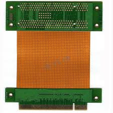
How do RF circuit boards ensure low signal attenuation?
To further reduce attenuation, signal routing on the RF circuit board is optimized. Keeping the transmission lines as short and direct as possible is essential for minimizing the distance the signal must travel, reducing the likelihood of attenuation due to resistance and other losses. Avoiding sharp bends and turns in the routing of the traces is also important. Sharp bends cause signal reflections and increased loss, as the signal encounters greater resistance when changing direction. Smooth, gradual bends in the traces help maintain a consistent impedance and reduce the possibility of signal degradation.
Via optimization is another technique used to minimize attenuation. Vias, which are vertical electrical connections between different layers of the circuit board, can introduce signal losses if not designed properly. When high-frequency signals pass through vias, they can experience increased attenuation due to the added inductance and resistance. To address this, advanced RF circuit boards use via-in-pad or blind/buried vias to reduce the length and resistance of the via connections. Additionally, minimizing the number of vias that the signal must pass through can significantly reduce signal losses, improving overall performance.
Power amplifiers are also integral to reducing signal attenuation in RF systems. RF circuit boards often include power amplifiers to boost signal strength before transmission, compensating for any attenuation that may have occurred earlier in the system. These amplifiers are designed to operate with minimal distortion and maintain signal integrity, even at high frequencies. By amplifying the signal before transmission, the circuit board ensures that the signal retains its strength over long distances or through challenging environments.
Shielding and grounding are essential practices for minimizing the effects of external interference, which can contribute to signal degradation. Proper grounding ensures that the RF circuit board can maintain stable operation by providing a low-resistance path for return currents. Additionally, shielding techniques, such as the use of ground planes and protective enclosures, help to prevent electromagnetic interference (EMI) that could cause signal attenuation and noise. The shielding protects the integrity of the signal as it travels through the board and reduces the risk of external factors causing unwanted signal loss.
Finally, frequency planning is crucial for minimizing signal attenuation. RF circuit boards are typically designed to operate within specific frequency ranges, and careful selection of operating frequencies helps to reduce signal attenuation. Higher frequencies are more prone to attenuation due to the increased interaction between the signal and the materials in the circuit board. By choosing lower frequencies for certain applications, designers can reduce the impact of attenuation and ensure better signal propagation.
In conclusion, RF circuit boards employ a variety of techniques to ensure low signal attenuation and maintain signal integrity. From selecting low-loss dielectric materials to optimizing signal routing and trace design, every aspect of the RF circuit board is carefully engineered to minimize signal loss. By reducing attenuation, RF circuit boards help to ensure that wireless communication systems perform efficiently, providing clear, strong signals over longer distances and in complex environments. As demand for high-performance communication systems continues to grow, the importance of minimizing signal attenuation in RF circuit boards will remain a key factor in the success of modern RF technologies.