
How Does HDI PCB Improve Signal Integrity?
In today’s fast-paced technological world, signal integrity is a critical factor in the performance of electronic devices. Signal integrity refers to the quality of an electrical signal as it travels through a circuit, and it’s crucial for ensuring that data is transmitted accurately and without interference. High-Density Interconnector (HDI) PCBs play a vital role in improving signal integrity, particularly in high-speed and high-performance electronic devices. In this article, we will explore how HDI PCBs enhance signal integrity and the specific features that contribute to their superior performance.
What is HDI PCB?
HDI PCBs are advanced circuit boards that use microvias, finer traces, and smaller components to achieve high-density routing in a compact space. Unlike traditional PCBs, which typically have larger vias and less dense routing, HDI PCBs allow for more complex and intricate designs, often featuring multiple layers, microvias, and advanced signal routing techniques. This capability is especially beneficial in modern devices such as smartphones, tablets, and medical equipment, where performance, space, and signal integrity are all critical.
Reduced Crosstalk and Noise
One of the primary ways in which hdi pcb improve signal integrity is by reducing crosstalk and noise. Crosstalk occurs when signals from adjacent traces interfere with each other, leading to data corruption or signal degradation. In traditional PCBs, this interference is often more pronounced due to the use of larger vias and less optimized routing. HDI PCBs, however, utilize microvias and more tightly packed traces, which reduces the chance of crosstalk.
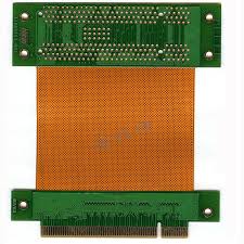
The ability to route signals more efficiently within a compact space minimizes the distance between traces, reducing the opportunity for interference. Additionally, HDI PCBs often employ advanced shielding techniques, such as ground planes and power planes, which further help in isolating sensitive signals from noise. These measures are particularly important in high-speed circuits, where maintaining the integrity of signals is paramount for reliable operation.
Shorter Signal Paths
HDI PCBs allow for shorter signal paths, which is another key factor in improving signal integrity. Traditional PCBs often require longer traces to connect components across different layers. These longer paths can lead to increased resistance, signal loss, and potential delays in signal transmission. In contrast, HDI PCBs use microvias to create direct connections between layers, significantly shortening the signal paths.
By reducing the length of signal traces, HDI PCBs decrease the chances of signal degradation, ensuring that high-speed signals travel with minimal loss. Shorter signal paths also reduce the time it takes for a signal to travel through the circuit, which is especially important for high-frequency applications. The result is faster, more reliable signal transmission, which is crucial for modern electronics like smartphones, computers, and communication devices.
Enhanced Grounding and Power Distribution
Another way that HDI PCBs improve signal integrity is through better grounding and power distribution. Signal integrity can be compromised if the power supply or ground plane is not well managed, as this can introduce noise and cause voltage fluctuations. HDI PCBs use advanced techniques to improve power distribution and provide clean, stable ground planes for signals to travel through.
In multi-layer HDI PCBs, dedicated power and ground layers can be incorporated, which help to stabilize the signal integrity. These layers are positioned between signal layers and provide a low-resistance path for current, reducing the potential for noise. Additionally, these dedicated power and ground planes ensure that high-speed signals have a consistent reference point, minimizing the effects of voltage fluctuations.
Impedance Control
Impedance control is a critical aspect of HDI PCB design that directly influences signal integrity. Impedance refers to the resistance a signal encounters as it travels through a trace. If the impedance is not controlled properly, signals can reflect or lose power, leading to distortion. HDI PCBs offer better control over impedance by using uniform trace widths and spacing, which ensures that the signal’s impedance remains constant throughout the entire PCB.
Through precise design techniques, HDI PCBs can maintain controlled impedance for high-speed signals, which is essential for applications such as data transmission and high-frequency communication. This level of control reduces signal reflections and ensures that signals are transmitted with high fidelity, which is essential for maintaining the overall integrity of the system.
Conclusion
HDI PCBs play a crucial role in improving signal integrity in modern electronics. Their ability to reduce crosstalk, shorten signal paths, enhance grounding, and control impedance makes them ideal for high-performance, high-speed devices. By optimizing the routing of signals and minimizing interference, HDI PCBs ensure that signals remain clear, strong, and reliable throughout the system. As electronics continue to evolve and become more complex, HDI PCBs will remain an essential technology for ensuring superior signal integrity and overall device performance.