
Rigid Flex Circuits Enable Multi-Layer
Rigid-flex circuits are multi-layered printed circuit boards that combine rigid and flexible board technologies to provide both structural integrity and a wide range of connectivity options. These circuits are useful in many different applications, from wearable devices to foldable laptops and tablets. Rigid flex boards can save space, reduce weight, and accommodate complex geometries in small spaces where traditional rigid PCBs cannot fit. They are also ideal for electronic systems that must withstand harsh conditions like mechanical shocks and vibrations.
Achieving high-quality rigid flex circuits layouts requires a comprehensive approach that encompasses several key best practices and considerations. Having an in-depth understanding of the stackup configuration, material selection, and manufacturability considerations is essential. This knowledge allows engineers to implement optimization strategies that yield high-quality rigid-flex designs tailored to the specific needs of their unique application.
Rigid flex layouts feature multiple layers of conductive copper with both rigid and flex portions. Rigid portions typically have one or more plated through holes, while the flex portion is comprised of unplated through-holes and buried vias. During fabrication, the exposed copper is developed using lithographic imaging, and chemical etching removes the patterned resist to expose conductor traces. The holes are mechanically drilled or laser-ablated, and blind and buried vias are used to connect the layers. The resulting structure is then laminated with an insulating substrate and etched with openings for mounting components and signal traces. The etching process leaves behind walls of copper, which are then plated with ENIG or immersion silver for soldering.
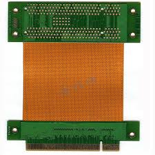
Rigid Flex Circuits Enable Multi-Layer Circuit Designs
A key challenge of the rigid-flex layout is to ensure that it can withstand repeated bending and flexing without suffering mechanical failure. This can be achieved through careful flexibility analysis, which focuses on the distribution of power, ground, and data signals between the rigid and flex sections. Signals should be positioned away from critical bending areas, and the design should incorporate thermal vias to minimize heat transfer between rigid and flex portions of the board. The rigid-flex layout should also incorporate tightly spaced ground vias and pads connected to the grounded layers, to limit EMI interference.
Other important design considerations for a rigid-flex layout include ensuring the stability of both the flexible and rigid sections of the circuit board. This can be accomplished by incorporating stiffeners along the flex portions of the board, which will help to stabilize the board during use and prevent damage to the traces or components. The rigid-flex layout should also include adequate air gaps to facilitate proper cooling and ventilation of the components and to allow for easy inspection and testing.
Rigid flex circuits can be designed with either a solid or cross-hatched copper shield layer to protect the circuits from electromagnetic interference (EMI). Solid copper shield layers offer increased strength and durability, but they may result in higher buckling in tighter bend radius settings. A cross-hatched copper layer offers better flexibility, but it may not provide sufficient EMI protection in some cases. In addition, the shielding layer should be arranged to avoid interference with the signal traces on the board.